
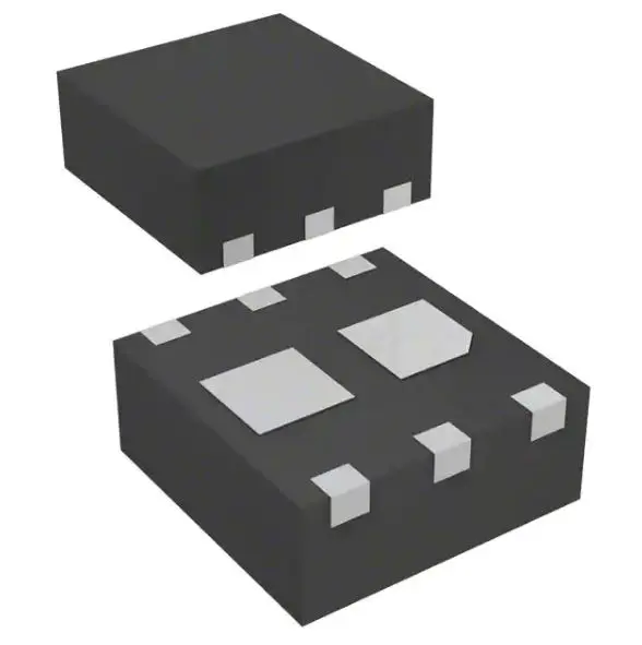
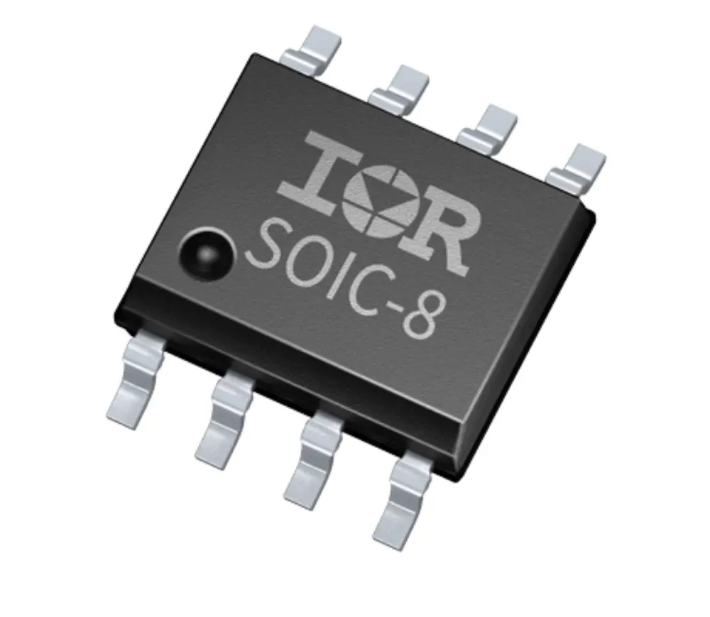
Descripción
This device is designed specifically as a single package solution for dual switching requirements in cellular handset and other ultra-portable applications. It features two independent N-Channel MOSFETs with low on-state resistance for minimum conduction losses. The MicroFET 2×2 offers exceptional thermal performance for its physical size and is well suited to linear mode applications.
2.9 A, 30 V
RDS(ON) = 123 mΩ @ VGS = 4.5 V
RDS(ON) = 140 mΩ @ VGS = 3.0 V
RDS(ON) = 163 mΩ @ VGS = 2.5 V
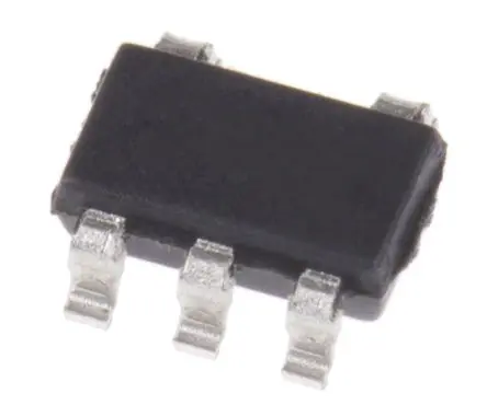
Low profile – 0.8 mm maximum – in the new package MicroFET 2×2 mm
HBM ESD protection level=1.8kV (Note 3)
Free from halogenated compounds and antimony oxides
Applications
This product is general usage and suitable for many different applications
| Atributo | Valor |
|---|---|
| Tipo de Canal | N |
| Corriente Máxima Continua de Drenaje | 2.9 A |
| Tensión Máxima Drenador-Fuente | 30 V |
| Tipo de Encapsulado | WDFN |
| Tipo de Montaje | Montaje superficial |
| Conteo de Pines | 6 |
| Resistencia Máxima Drenador-Fuente | 268 mΩ |
| Modo de Canal | Mejora |
| Tensión de umbral de puerta máxima | 1.5V |
| Tensión de umbral de puerta mínima | 0.4V |
| Disipación de Potencia Máxima | 1.5 W |
| Tensión Máxima Puerta-Fuente | ±12 V |
| Temperatura Máxima de Funcionamiento | +150 °C |
| Ancho | 2mm |
| Número de Elementos por Chip | 2 |
| Carga Típica de Puerta @ Vgs | 2.4 nC @ 4.5 V |
| Longitud | 2mm |
| Altura | 0.75mm |
| Tensión de diodo directa | 1.2V |
| Temperatura de Funcionamiento Mínima | -55 °C |

Valoraciones
No hay valoraciones aún.